From Silicon to Chips
How sand becomes a GPU — transistors, lithography, process nodes, die size, packaging, HBM stacking, and why chip economics shape AI infrastructure.
The GPU sitting in your server was once sand. Understanding the journey from silicon to finished chip explains why GPUs cost what they cost, why supply is constrained, why NVIDIA went dual-die with Blackwell, and why HBM is expensive. These aren’t trivia — they’re the physical constraints that shape every AI infrastructure decision.
1. Transistors: The Atomic Unit of Compute
A transistor is a switch — it’s either on (1) or off (0). That’s it. Every computation ever performed by a computer, from “1+1” to “generate a 10,000-word essay,” reduces to billions of these switches flipping on and off.
How a Transistor Works
A modern transistor (FinFET or GAA) has three terminals:
- Gate: the control signal (voltage on or off)
- Source and Drain: current flows between them when the gate is on
        Gate
         |
    ┌────┴────┐
    │  Oxide  │
Source ───┤ Channel ├─── Drain
    │         │
    └─────────┘
When the gate voltage is high → channel conducts → current flows (state: 1). When the gate voltage is low → channel blocks → no current (state: 0).
Scale: An H100 GPU has 80 billion transistors. Each is roughly 5 nanometers wide — about 10 atoms across. For comparison, a human hair is ~80,000 nm wide.
2. From Transistors to Logic
Logic Gates
Combinations of transistors form logic gates — the building blocks of all computation:
| Gate | Function | Transistors |
|---|---|---|
| NOT | Invert: 0→1, 1→0 | 2 |
| AND | Output 1 only if both inputs are 1 | 6 |
| OR | Output 1 if either input is 1 | 6 |
| XOR | Output 1 if inputs differ | 8-12 |
From Gates to Arithmetic
Gates combine into higher-level circuits:
Logic gates → Adder (adds two numbers)
           → Multiplier (multiplies two numbers)
           → ALU (Arithmetic Logic Unit — the core compute unit)
           → FMA unit (Fused Multiply-Add: a×b+c in one operation)
           → Tensor Core (matrix of FMA units working together)
A single FMA (fused multiply-add) computes in one operation — this is the atomic operation of deep learning. Every matrix multiplication is millions of FMAs. A Tensor Core is a grid of FMA units that operate in lockstep on small matrix tiles.
Key insight: The entire AI infrastructure stack — from FlashAttention to distributed training — ultimately exists to keep these FMA units fed with data and busy with work.
3. How Chips Are Manufactured
The Fabrication Process
Turning a chip design into physical silicon takes ~3 months and involves ~1,000 steps:
Step 1: Wafer preparation
- Start with a 300mm (12-inch) silicon wafer — a near-perfect crystal grown from molten sand
- The wafer is polished to atomic-level flatness
Step 2: Lithography (the critical step)
- Coat the wafer with photoresist (light-sensitive material)
- Project the circuit pattern onto the wafer using extreme ultraviolet (EUV) light
- The light creates the pattern of transistors at nanometer scale
- This step is repeated ~80-100 times for different layers
Step 3: Etching and deposition
- Chemical processes remove material where the light exposed it
- Deposit metal layers for wiring between transistors
- Build up ~15-20 layers of interconnects
Step 4: Testing and dicing
- Test every die on the wafer
- Cut the wafer into individual dies
- Package the working dies
Process Nodes: What “5nm” Means
When NVIDIA says the H100 uses “TSMC 4N” (a variant of 4nm), this refers to the process node — roughly the minimum feature size. Smaller nodes mean:
| Node | Transistor density | Used by | Benefit |
|---|---|---|---|
| 7nm | ~90M transistors/mm² | A100 | Baseline |
| 5nm/4nm | ~130M transistors/mm² | H100 | ~1.5× density, lower power |
| 3nm | ~200M transistors/mm² | Apple M3, future GPUs | ~2× density |
“nm” is marketing, not physics. Modern “5nm” transistors aren’t actually 5nm in any measurable dimension. The number is a node name, not a measurement. What matters: each node delivers ~1.5× transistor density and ~15-30% power reduction vs the previous node.
TSMC: The Bottleneck
TSMC (Taiwan Semiconductor Manufacturing Company) fabricates ~90% of the world’s advanced AI chips, including every NVIDIA GPU. There is no alternative at the leading edge — Samsung and Intel foundries are years behind for AI chip production.
This concentration matters for AI infrastructure: When TSMC’s 4nm capacity is sold out, you can’t get H100s regardless of price. The global GPU shortage of 2023-2024 was fundamentally a TSMC capacity constraint.
4. Die Size and Yield
Why Die Size Matters
A GPU’s die is the piece of silicon cut from the wafer. Larger die = more transistors = more compute, but:
| Larger die | Smaller die |
|---|---|
| ✅ More transistors, higher performance | ✅ More dies per wafer, lower cost |
| ✅ More on-chip memory (cache, registers) | ✅ Higher yield (fewer defects per die) |
| ❌ Fewer dies per wafer | ❌ Less compute per die |
| ❌ Lower yield (defects more likely to hit) | ❌ Need multi-chip designs for high perf |
Yield: The Economics of Defects
Every wafer has random defects (particles, crystal imperfections). If a defect lands on a die, that die is dead.
For a 300mm wafer:
- Small die (100mm²): ~600 dies per wafer. One defect kills 1/600 = 0.17% loss
- Large die (800mm²): ~60 dies per wafer. One defect kills 1/60 = 1.7% loss
H100 die size: ~814 mm² — near the reticle limit (the maximum area the lithography machine can expose in one shot, ~858 mm²). This is as big as a single die can physically be.
This is why:
- H100 is expensive ($25K-40K): huge die = low yield = high cost per working chip
- Blackwell B200 uses dual-die (two ~400mm² dies): each die has much higher yield, then they’re connected with a 10 TB/s link. Two cheaper dies > one expensive die.
- Consumer GPUs (RTX 4090) use smaller dies (~600mm²) with defective portions disabled (“binning”)
5. Packaging: Connecting Die to Memory
The raw die is useless alone — it needs to be packaged with memory, power delivery, and I/O connections.
Standard Packaging
Traditional: die mounted on a substrate with wire bonds or flip-chip bumps. Memory chips (GDDR) are separate chips on the PCB.
Advanced Packaging for AI (CoWoS)
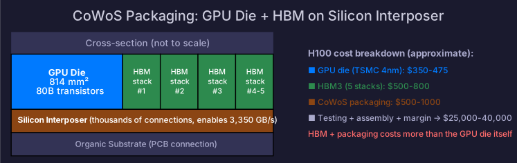
Modern AI GPUs use CoWoS (Chip-on-Wafer-on-Substrate) — TSMC’s advanced packaging that places the GPU die and HBM stacks side by side on a silicon interposer:
┌──────────────────────────────────────────────┐
│              Silicon Interposer               │
│  ┌────────┐  ┌────┐ ┌────┐ ┌────┐ ┌────┐   │
│  │  GPU   │  │HBM │ │HBM │ │HBM │ │HBM │   │
│  │  Die   │  │ #1 │ │ #2 │ │ #3 │ │ #4 │   │
│  │        │  │    │ │    │ │    │ │    │   │
│  │ 814mm² │  │20GB│ │20GB│ │20GB│ │20GB│   │
│  └────────┘  └────┘ └────┘ └────┘ └────┘   │
│              (HBM3: 4-high stack each)        │
└──────────────────────────────────────────────┘
                      │
              ┌───────┴──────┐
              │  Substrate    │
              └──────────────┘
Why CoWoS matters for AI:
- The silicon interposer provides thousands of connections between GPU and HBM — enabling 3,350 GB/s bandwidth (H100)
- Traditional PCB traces can’t achieve this bandwidth
- CoWoS capacity at TSMC is a separate bottleneck from wafer fabrication — even if TSMC makes enough GPU dies, insufficient CoWoS capacity limits total GPU production
HBM: Stacked Memory
HBM (High Bandwidth Memory) achieves high bandwidth by stacking DRAM dies vertically:
| HBM Generation | Stacks | Capacity per stack | Bandwidth per stack |
|---|---|---|---|
| HBM2e (A100) | 4-8 high | 8-16 GB | ~410 GB/s |
| HBM3 (H100) | 8 high | 16 GB | ~670 GB/s |
| HBM3e (B200) | 12 high | 24 GB | ~1,000 GB/s |
Each stack connects to the GPU through thousands of through-silicon vias (TSVs) — vertical holes drilled through the silicon. More stacks = more capacity but also taller packages and harder thermal management.
6. From Fab to Data Center: The Supply Chain
The journey from sand to running AI workloads:
Sand (SiO₂)
  → Silicon ingot (crystal growth, ~1 month)
  → 300mm wafer (slicing, polishing)
  → TSMC fab (lithography, ~3 months)
  → Working dies (testing, dicing)
  → CoWoS packaging with HBM (~1 month)
  → NVIDIA module (PCB, power, NVLink connectors)
  → Server OEM (Dell, Supermicro) or DGX assembly
  → Data center (installation, networking, cooling)
  → Your training job starts

Total lead time: 6-12 months from wafer start to running workloads
Why GPUs Are Expensive
| Cost factor | Impact |
|---|---|
| TSMC fabrication (4nm) | ~350-475 per working die |
| HBM3 (5 stacks × 16GB) | ~$500-800 per GPU worth of HBM |
| CoWoS packaging | ~$500-1000 (complex process, limited capacity) |
| Testing, module assembly | ~$200-500 |
| NVIDIA margin | ~40-60% gross margin |
| Total (H100 SXM) | ~$25,000-40,000 |
The single largest cost driver is not the GPU die itself — it’s the HBM and advanced packaging that together cost more than the compute silicon.
7. Why This Matters for AI Infrastructure
| Physical constraint | Infrastructure consequence |
|---|---|
| Die size at reticle limit | Multi-die designs (Blackwell), chiplets |
| HBM bandwidth limits | Memory-bound inference, KV cache optimization |
| CoWoS capacity | GPU supply constraints, long procurement lead times |
| Power scaling (TDP: 300W → 1000W) | Liquid cooling required, data center power limits |
| TSMC concentration | Geopolitical risk, supply chain fragility |
| Process node cadence (~2 years) | GPU refresh cycles, hardware procurement planning |
Understanding chip economics answers questions like:
- “Why can’t we just buy more GPUs?” → CoWoS/HBM supply constraints
- “Why are H100s so expensive?” → Huge die + HBM + CoWoS + NVIDIA margin
- “Why did Blackwell go dual-die?” → Better yield at smaller die size
- “When will the next GPU generation be available?” → TSMC process node cadence
Self-Check
- Explain what a transistor does and why billions are needed for AI compute
- Explain FMA and why it’s the atomic operation of deep learning
- Explain what happens during chip lithography
- Explain why smaller process nodes (5nm vs 7nm) matter for GPUs
- Explain why larger dies have lower yield and higher cost
- Explain CoWoS packaging and why it’s needed for HBM bandwidth
- Explain why TSMC is a bottleneck for AI GPU supply
- Explain the cost breakdown of an H100
References
- How a CPU Works — Ben Eater (YouTube) — building a CPU from logic gates
- TSMC Technology Overview
- Asianometry — Semiconductor Industry (YouTube) — excellent semiconductor analysis
- SemiAnalysis — GPU Supply Chain Analysis
- Chips and Cheese — GPU Architecture Deep Dives
- Putting the “You” in CPU — interactive guide from transistors to execution