GPU Architecture
CPU vs GPU design philosophy, the SM hierarchy, warps, and the memory pyramid — the hardware foundation for everything in AI infrastructure.
The GPU is the engine of the large model era — training a 100-billion-parameter LLM may require thousands of GPUs running for months, and inference throughput and latency are directly determined by GPU utilization efficiency. For AI infrastructure engineers, understanding the GPU is not optional — it is the hardware foundation for every subsequent optimization (kernels, parallelism, scheduling).
1. CPU vs GPU: Why Deep Learning Chose the GPU
Imagine you need to grade 10,000 multiple-choice exams. The CPU approach is to hire one highly experienced grader — fast, able to handle complex question types, but can only grade one paper at a time. The GPU approach is to hire 10,000 temporary workers, each capable of only checking answers against an answer key, but all working simultaneously — finished in 1 second.
This is the core difference between latency-oriented and throughput-oriented design.
The Fundamental Architectural Difference
| Dimension | CPU | GPU |
|---|---|---|
| Design goal | Low latency for complex tasks | High throughput for massive simple tasks |
| Core count | A few to dozens of “big” cores | Thousands to tens of thousands of “small” cores |
| Single-core capability | Strong (branch prediction, out-of-order execution) | Weak (simple ALUs, in-order execution) |
| Cache ratio | Majority of chip area | Small fraction of chip area |
| Control logic | Complex (out-of-order, branch predictor) | Simple (many cores share control units) |
| Memory bandwidth | ~300–400 GB/s (8-channel DDR5 server) | Extremely high (HBM3 ~3 TB/s) |
| Best suited for | Serial logic, OS, networking | Matrix operations, data parallelism |
Why Deep Learning Is a Natural Fit
At the lowest level, deep learning is massive matrix multiplications and element-wise operations:
- Forward pass: every layer is — matrix multiplication
- Backward pass: computing gradients is still matrix multiplication ()
- Attention: — matrix multiplication at its core
These operations share two critical characteristics:
- Extreme data parallelism: each element’s computation is independent — naturally distributable across cores
- Regular computation patterns: no complex branching — all threads execute the same instruction
An H100 GPU delivers ~989 TFLOPS of FP16 compute, while a high-end server CPU typically achieves single-digit TFLOPS in FP16. The gap is over two orders of magnitude.
2. GPU Hardware Hierarchy
Taking NVIDIA GPUs as an example, compute cores are organized hierarchically:
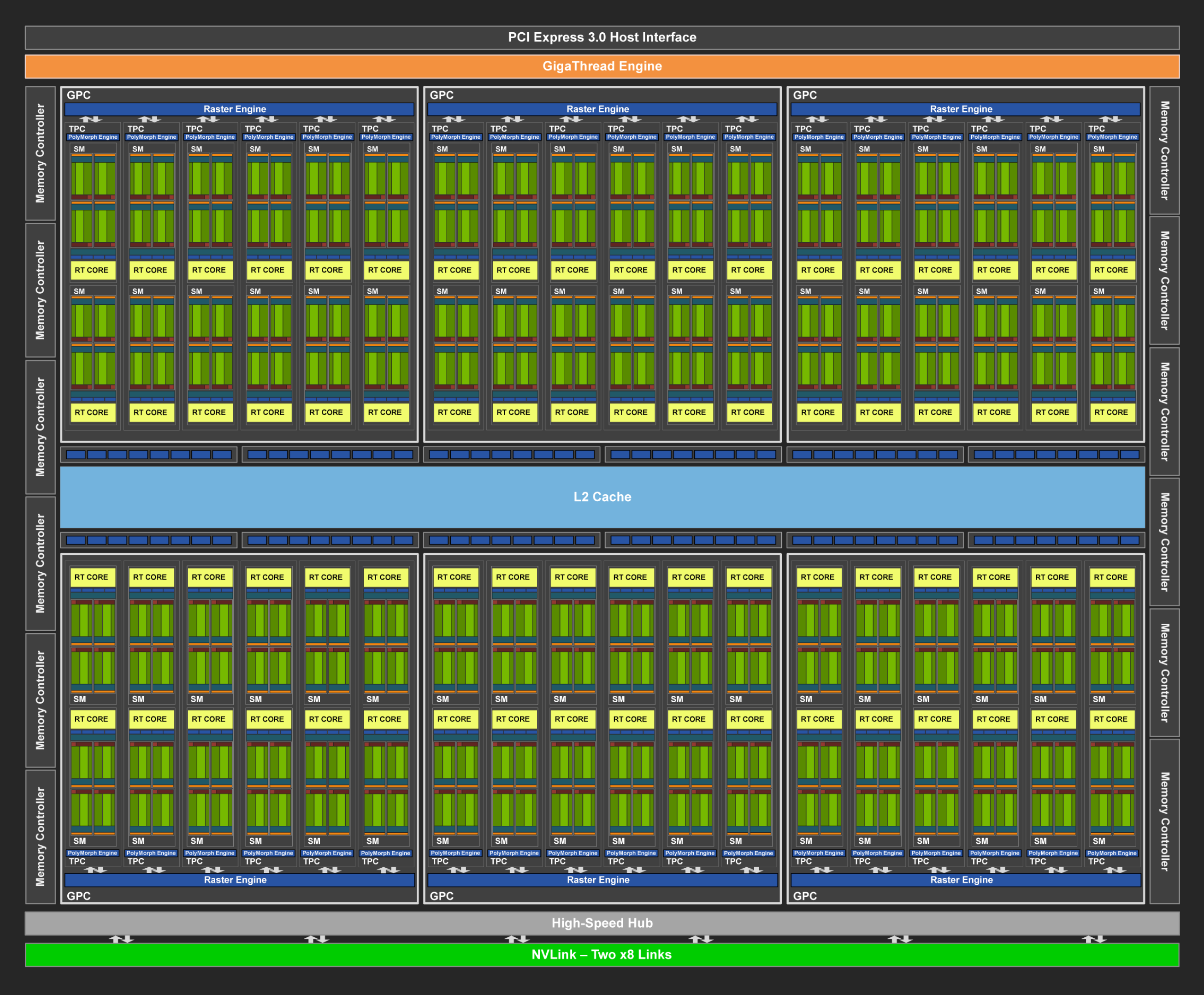
GPU Chip
├── GPC (Graphics Processing Cluster)      ← "Division"
│   ├── TPC (Texture Processing Cluster)   ← "Department"
│   │   └── SM (Streaming Multiprocessor)  ← "Team" — the basic scheduling unit
│   │       ├── CUDA Core × N             ← FP32/INT32 operations
│   │       ├── Tensor Core × M           ← Matrix operations
│   │       ├── SFU                        ← sin/cos/exp
│   │       ├── Register File              ← Fastest storage
│   │       └── Shared Memory / L1         ← SM-shared high-speed storage
├── L2 Cache (globally shared)
└── Memory Controller → HBM (device memory)
SM: The Basic Scheduling Unit
The SM is the key to understanding GPU architecture — all thread scheduling and execution happens at the SM level.
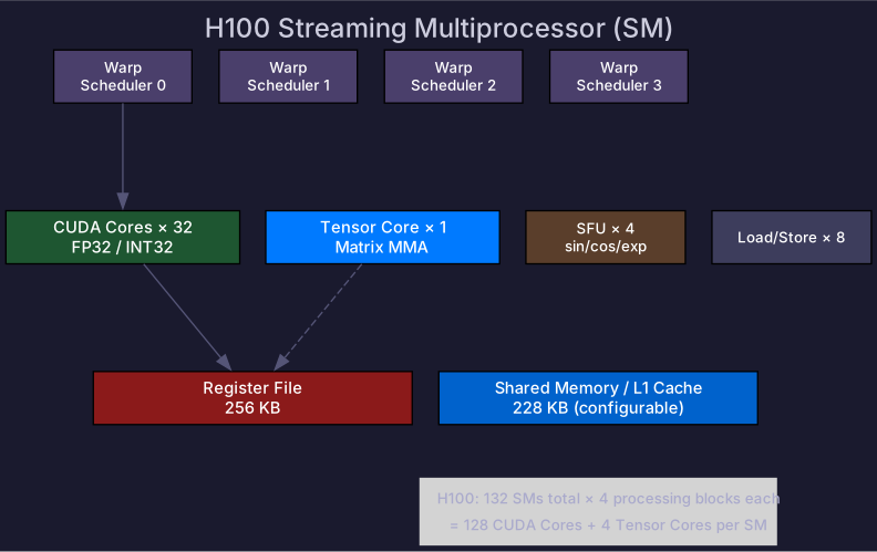
Taking the H100’s SM as an example, each SM contains:
| Component | Count | Function |
|---|---|---|
| CUDA Cores (FP32) | 128 | Floating-point and integer operations |
| Tensor Cores (4th gen) | 4 | Matrix multiply-accumulate (MMA) |
| Load/Store Units | 32 | Memory read/write |
| SFU | 16 | Transcendental functions (sin, cos, exp) |
| Warp Schedulers | 4 | Dispatch 4 warps per cycle |
| Register File | 256 KB | Thread-private registers |
| Shared Memory / L1 Cache | 228 KB | Configurable split between shared memory and L1 |
Key point: The SM is the smallest granularity of resource allocation. A thread block is scheduled onto one SM, and all thread blocks on that SM share its registers, shared memory, and other resources.
Warp: The Minimum Execution Unit
GPUs don’t execute one thread at a time — they execute in warps of 32 threads in lockstep, all executing the same instruction.
Warp (32 threads)
├── Thread 0:  execute add r1, r2, r3
├── Thread 1:  execute add r1, r2, r3  (same instruction, different data)
├── ...
└── Thread 31: execute add r1, r2, r3
This execution model is called SIMT (Single Instruction, Multiple Threads) — NVIDIA’s extension of SIMD.
Warning: If threads within a warp hit a branch (if-else), threads taking different paths are masked, causing some to sit idle. This is warp divergence — a performance killer that GPU programmers must avoid.
3. Memory Hierarchy & Bandwidth
No matter how fast GPU compute is, it’s wasted if data can’t be fed fast enough. In AI workloads, memory bandwidth often becomes the bottleneck before compute — this is why the AI infra community says “Memory is the new compute.”
GPU Memory Pyramid
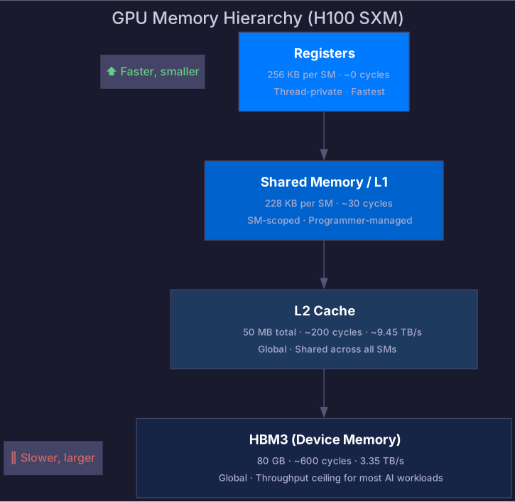
Using the H100 SXM as an example:
| Level | Capacity | Bandwidth | Latency | Scope |
|---|---|---|---|---|
| Registers | 256 KB per SM | — | ~0 cycles | Thread-private |
| Shared Memory / L1 | 228 KB per SM | ~240 GB/s per SM | ~30 cycles | SM-scoped |
| L2 Cache | ~50 MB total | ~9.45 TB/s aggregate | ~200 cycles | All SMs |
| HBM3 | 80 GB | 3.35 TB/s | ~600 cycles | Global |
Shared memory bandwidth of ~240 GB/s is per SM. Across all 132 SMs, the aggregate is much higher — but each SM only sees its own local bandwidth.
HBM: High Bandwidth Memory
Traditional GDDR memory is like a single-lane highway. HBM stacks thousands of lanes together via a silicon interposer, achieving massive bandwidth:
| Memory Type | Representative GPU | Bandwidth | Capacity |
|---|---|---|---|
| GDDR6X | RTX 4090 | 1,008 GB/s | 24 GB |
| HBM2e | A100 | 2,039 GB/s | 80 GB |
| HBM3 | H100 | 3,350 GB/s | 80 GB |
| HBM3e | B200 | 8,000 GB/s | 192 GB |
From A100 to B200, memory bandwidth has grown nearly 4×. This matters enormously for LLM inference — the decode phase is a classic memory-bound task.
Roofline Model: Compute vs Bandwidth
To determine whether a task is compute-bound or memory-bound, use arithmetic intensity:
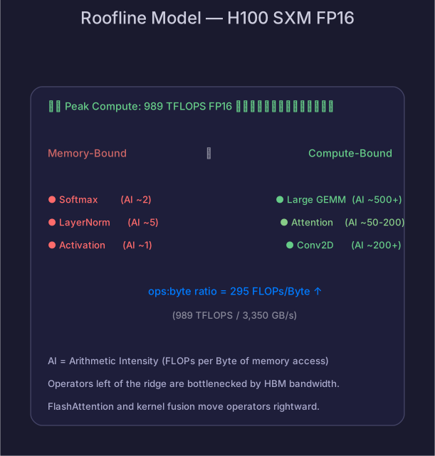
For the H100 SXM:
- FP16 compute: 989 TFLOPS
- HBM3 bandwidth: 3,350 GB/s
- ops:byte ratio = FLOPs/Byte
This means: for every byte read from HBM, the kernel must perform at least 295 FP16 operations to fully utilize compute. Most deep learning operators (attention, LayerNorm, activations) fall far below this — they are memory-bound. This is why FlashAttention and kernel fusion are so critical: they reduce memory access to increase arithmetic intensity.
Self-Check
- Explain the core architectural difference between CPUs and GPUs
- Draw the GPU hierarchy (GPC → SM → CUDA Core / Tensor Core)
- Explain warps and why warp divergence hurts performance
- Name GPU memory levels with approximate capacity and latency for H100
- Use the roofline model to determine if an operator is compute-bound or memory-bound
- Calculate the ops:byte ratio for a given GPU